In our previous lesson, we built the SR Latch. While it is an excellent way to store a bit, it has a significant weakness: the "invalid state." If both the Set and Reset inputs are turned on at the same time, the circuit becomes unpredictable.
The D Latch (Data Latch) is the solution to this problem. It is one of the most important building blocks in digital electronics because it simplifies how we store data. Instead of managing two separate Set and Reset signals, we use a single data input. This ensures that the circuit always receives a clear, valid instruction, making our memory much more reliable for complex computers.
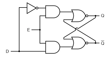
The D in D Latch stands for Data. To fix the ambiguity of the SR Latch, we use a NOT gate to connect the internal Set and Reset paths.
In the circuit you will build, the input D is split into two paths:
- One path goes through a
NOT gatebefore reaching the storage part of the circuit. - The other path goes directly toward the storage part.
Because of the NOT gate, the two internal signals will always be opposites. If D is 1, the other path must be 0. If D is 0, the other path must be 1. This "forces a choice" and completely removes the possibility of both inputs being 1 at the same time. This simple addition ensures that the circuit is always in a stable, predictable state.
While having a data input is helpful, we do not always want our memory to change the moment the D input flickers. We need a way to tell the circuit: "Okay, listen to the data now," or "Ignore the data and keep what you have."
We do this by adding an Enable (E) input. In your circuit, the E signal is connected to two AND gates. These AND gates act as digital gatekeepers.
- When E is 0 (Low): The outputs of the
AND gatesare forced to0, regardless of what theDinput is doing. This puts the internalSR Latchinto "Hold" mode, keeping the stored bit safe. - When E is 1 (High): The
AND gates"open," allowing theDsignal to pass through and update the stored value.
Think of the Enable pin as the "Save" button in a text editor. Your changes only become permanent when you decide it is time to save them.
The D Latch is described as level-sensitive. This means that as long as the Enable pin is held at a high voltage (1), the output Q will follow the input D. If D changes while E is high, the output changes immediately. This state is often called "transparency" because you can see the input move straight through to the output.
We can visualize this behavior using a waveform, which is a graph showing how signals change over time.
As you can see in the table, the only time the memory actually changes is when E is 1. Once E returns to 0, the value is locked in, regardless of what happens to D.
In this lesson, we refined our understanding of digital memory by looking at the D Latch. Here is a quick summary of how it works:
- D (Data): The value we want to store (
0or1). - E (Enable): The control signal that determines if the latch is "open" or "locked."
- The NOT Gate: Prevents the "invalid state" by ensuring internal signals are always opposites.
- Logic: If
E = 1, thenQ = D. IfE = 0,Qstays at its last stored value.
In the upcoming practice, you will head into the CodeSignal IDE to construct a D Latch from scratch. You will use a NOT gate, two AND gates, and the cross-coupled NOR gates you learned about in the SR Latch lesson. Pay close attention to how the Enable signal controls the flow of data into your memory cell!
